
PORTFOLIO PREVIEW · Project images are illustrative; original media is being added
AFFAN IMAN · ENGINEERING PORTFOLIO

Custom IC layout.
Every layer matters.

I’m Affan Iman, a Mechatronics graduate focused on custom IC layout. My hands-on experience spans 40 nm standard cells, 28 nm analog layout, physical verification, and SKILL automation.

40 nm standard cells28 nm analog layoutSKILL automation
PENANG, MALAYSIA

Custom IC layout · Mechatronics

1 / The waferPatterned silicon
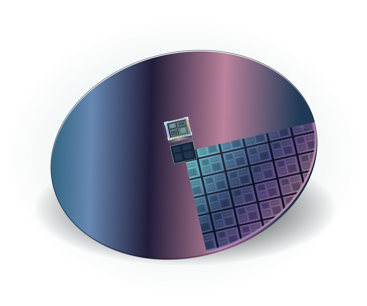
Conceptual iridescent silicon wafer with a grid of dies and one highlighted dieConceptual wafer, die, interconnect, devices, and transistor. Choose a stage using the buttons below.Conceptual silicon · not to scale

Scroll from the wafer to a single transistor

Explore freely
0%

1 / The wafer

A patterned silicon wafer contains many individual dies. Follow one die into its physical layers.

EDA TOOLS

Virtuoso
Calibre
Custom Compiler

PROCESS-NODE EXPERIENCE

40 nmPlanar
32 nmPlanar
28 nmPlanar
14 nmFinFET
INTERESTS & LEARNING PATH

Growing towards
layout mastery.

From proven layout foundations to deeper circuit knowledge, advanced devices and a more efficient workflow.

NEXT LEARNING BRANCHES Tap a topic to explore

Advanced nodes

FinFET → GAAFETExplore learning path

Learning focus

Extend my SAED14 nm FinFET training towards smaller process nodes and gate-all-around devices.

Layout perspective

Fin quantisation, restricted routing, device orientation, local interconnect and PDK-specific design rules.

Planned exercise

Compare one standard-cell layout across available educational PDKs; document which constraints change. GAAFET and smaller-node work are learning goals.

Automation & workflow

SKILL · scripting · repeatabilityExplore learning path

Learning focus

Build on existing SKILL utilities to make repeated layout tasks faster and more consistent.

Layout perspective

Bindkeys, instance labels, ruler generation, layer operations, reusable checks and clear revision records.

Planned exercise

Extend one utility with input validation, an undo-safe workflow and a repeatable before/after demonstration.

SerDes

High-speed links & clock recoveryExplore learning path

Learning focus

Study serial-link architecture, transmitter and receiver blocks, clock and data recovery (CDR), jitter, and equalisation.

Layout perspective

Differential symmetry, sensitive-node isolation, coupling, and parasitic-aware routing.

Planned exercise

Draw a transmitter-to-receiver signal path, then compare matched and mismatched differential-route examples.

PLL

Frequency synthesis & phase controlExplore learning path

Learning focus

Deepen understanding of phase/frequency detectors, charge pumps, loop filters, voltage-controlled oscillators (VCOs), dividers, and loop behaviour.

Layout perspective

Charge-pump matching, oscillator isolation, supply noise, and sensitive control-voltage routing.

Planned exercise

Build a block-level PLL model and study the trade-off between settling behaviour and jitter filtering.

DLL

Delay control & clock alignmentExplore learning path

Learning focus

Study delay-locked loops, phase detection, controlled delay lines, lock range, and clock deskew.

Layout perspective

Consistent delay-cell placement, balanced clock routes, loading, and supply sensitivity.

Planned exercise

Model a delay chain and observe how feedback aligns its output clock with a reference.

Memory

SRAM, DRAM, ROM & HBMExplore learning path

Learning focus

Strengthen memory fundamentals: 6T SRAM read/write operation and stability, DRAM charge storage and refresh, ROM organisation, and HBM architecture.

Layout perspective

Bitcell regularity, wordline/bitline loading, sense-amplifier matching, and array/periphery interfaces.

Planned exercise

Start with a 6T SRAM schematic and operating-state study, then explore a small array and its peripheral blocks.

RFIC

Low-noise amplifiers & mixersExplore learning path

Learning focus

Develop understanding of LNAs, mixers, variable-gain amplifiers, impedance matching, noise, and linearity.

Layout perspective

Differential routing, shielding and return paths, substrate coupling, and passive-device placement.

Planned exercise

Study an LNA schematic and annotate its signal path, bias network, and layout-sensitive connections.

Layout Verification

PEX, post-layout behaviour & reliabilityExplore learning path

Learning focus

Build on DRC/LVS experience towards parasitic extraction (PEX), schematic-versus-extracted comparison, and electromigration/IR-drop awareness.

Layout perspective

Relate routing and device placement to circuit behaviour, matching, and robust power connections.

Planned exercise

When extraction tools and a suitable PDK are available, compare a small analog block before and after extraction and document the differences.

A learning roadmap, not a proficiency score. Advanced-node, RF and high-speed blocks are development goals; completed work is shown in the IC gallery.

Long-term goalContribute to a tapeout, connecting layout decisions with extracted circuit performance and sign-off requirements.

EXPERIENCE THAT SHAPES THE WORK

From foundations
to analog layout.

Full background ↗
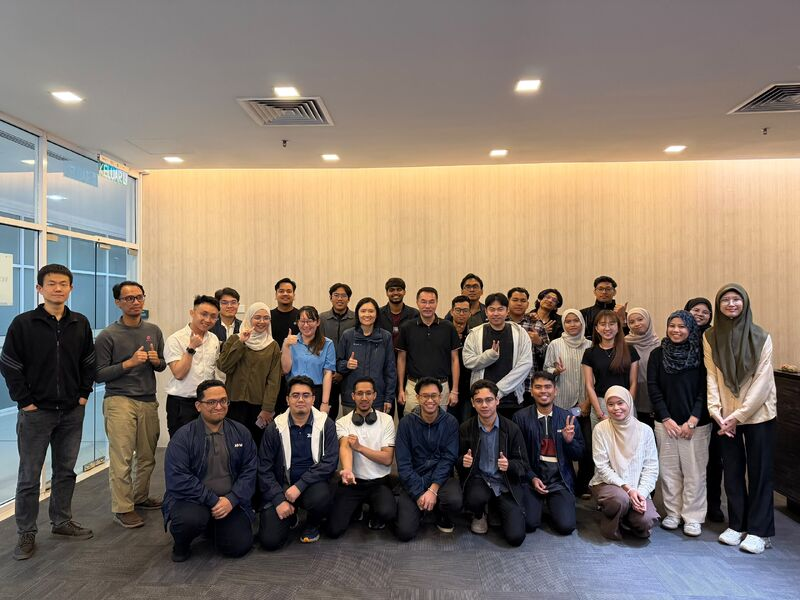
Vchip Technology training group photographView full photo ↗
Jun 2026 — Present

Custom Layout Engineer Trainee

Vchip Technology · Penang

40 nm · RunPeng

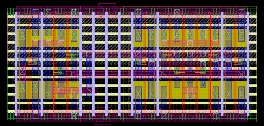
Logic-gate layouts, including long-gate variants, half adders and full adders. Device placement, routing and layout iteration.

28 nm · TSMC

Analog layout across two project sequences:

  • Bandgap op-amp → bandgap reference.
  • Separate bandgap reference → LDO → LDO_Bandgap TOP.

Completed with DRC-clean and LVS-matched results. Iteratively optimised placement, matching, routing and layout organisation.

Cadence VirtuosoCalibre DRC/LVSLayout optimisation
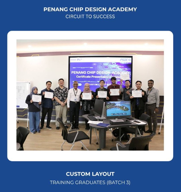
PSDC Penang Chip Design Academy custom layout training graduates, batch 3View full photo ↗
May — Jun 2026

IC Design Custom Layout

Penang Skills Development Centre

32 nm · SAED32

Digital logic gates, SRAM exercises and analog matching techniques, including interdigitated and common-centroid placement.

14 nm FinFET · SAED14

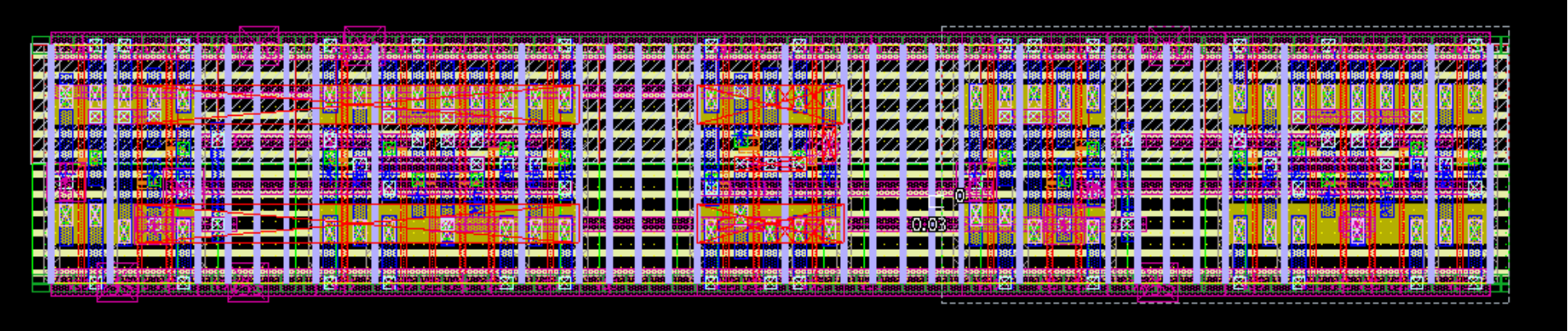
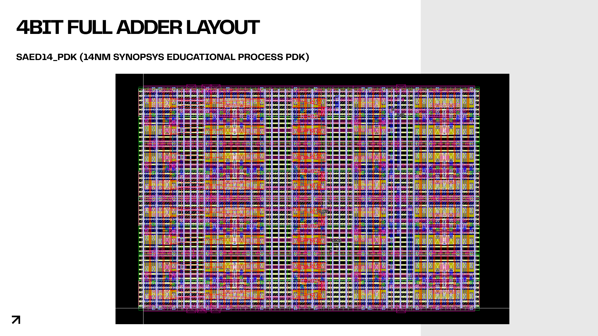
Half-adder and full-adder layouts, extended into hierarchical 4-bit, 8-bit and 16-bit full adders.

Practice in schematic-to-layout connectivity, cell hierarchy and physical verification using educational PDKs.

Synopsys Custom CompilerIC ValidatorSAED32 / SAED14
TECHNICAL TOOLKIT

Built through
hands-on layout.

Specific capabilities behind my standard-cell, analog and verification work.

Schematic-driven floorplanning

Translate circuit hierarchy into device groups, signal flow and routing space. Plan sensitive nodes, supply connections and block interfaces before detailed routing.

Bandgap / LDO

Analog device matching

Interdigitated and common-centroid placement, symmetry, dummies and consistent orientation. Prioritise differential pairs, current mirrors, resistor arrays and BJT placement.

Matching / layout-dependent effects

Digital & FinFET layout

40 nm logic and adder layouts; SAED32 digital and SRAM exercises; SAED14 FinFET half/full adders and hierarchical 4-, 8- and 16-bit adders.

40 nm / 32 nm / 14 nm

Physical verification

Interpret DRC markers, trace LVS mismatches and review connectivity against the schematic. Resolve violations, rerun checks and track changes through layout iterations.

Calibre / IC Validator

Analog integration & optimisation

28 nm bandgap and LDO integration, inter-block routing, guard rings and power/ground continuity. Refine placement and routing while preserving matching intent.

28 nm analog

SKILL & efficient workflow

Practical utilities for bindkeys, cross rulers, instance labels and metal-layer operations. Use repeatable editing steps and review generated results in the layout.

Cadence SKILL / Linux
Image guide — see what to upload for this section
PREPARING THE PORTFOLIO

Your image guide.

Examples for choosing your project photos, layout screenshots, portrait, and credentials.

IC Design · Layout screenshots, automation examples, and a workstation photo.
IC DESIGN · PROJECT COVER

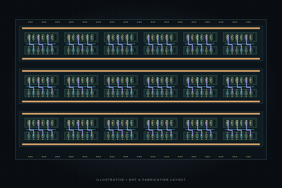
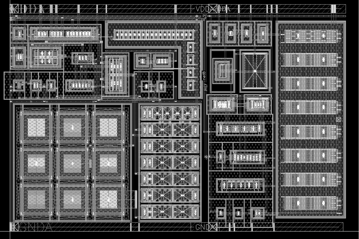
Standard-cell layout

One gate, one clear view.

16:10

Add a clear, shareable screenshot of your inverter, logic gate, or adder layout. Crop tightly enough to see the layers.

Use a direct screenshot instead of photographing your screen.
IC DESIGN · ANALOG PROJECT

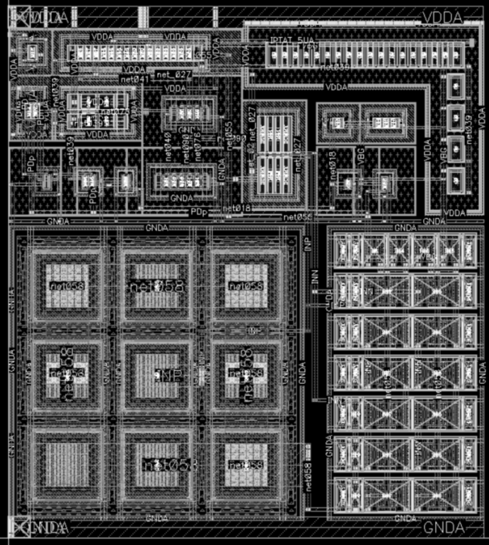
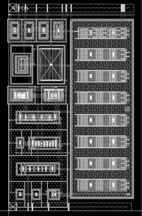
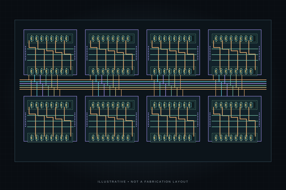
Analog layout overview

Show the overall organization.

16:10

Use an approved overview of a bandgap, op-amp, or LDO layout. A conceptual floorplan also works when the actual layout cannot be shared.

Remove confidential names and use only images you are allowed to show.
IC DESIGN · AUTOMATION

SKILL automation

Show the before and after.

16:9

Place two screenshots side by side to show what your script changes: labels, metal layers, bindkeys, or a repeated layout task.

Use the same zoom and crop in both screenshots. Keep text readable.
IC DESIGN · WORKING PROCESS

You at your workstation
Show the person behind the work.

16:9

Use a landscape photo of you working at a tidy engineering desk. An over-the-shoulder angle works well.

Keep the monitor content shareable and leave space around the subject.

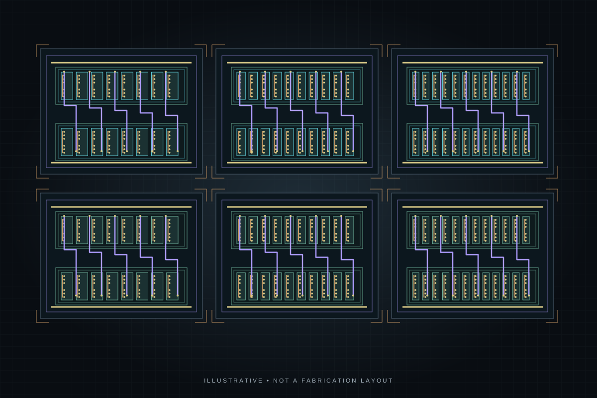
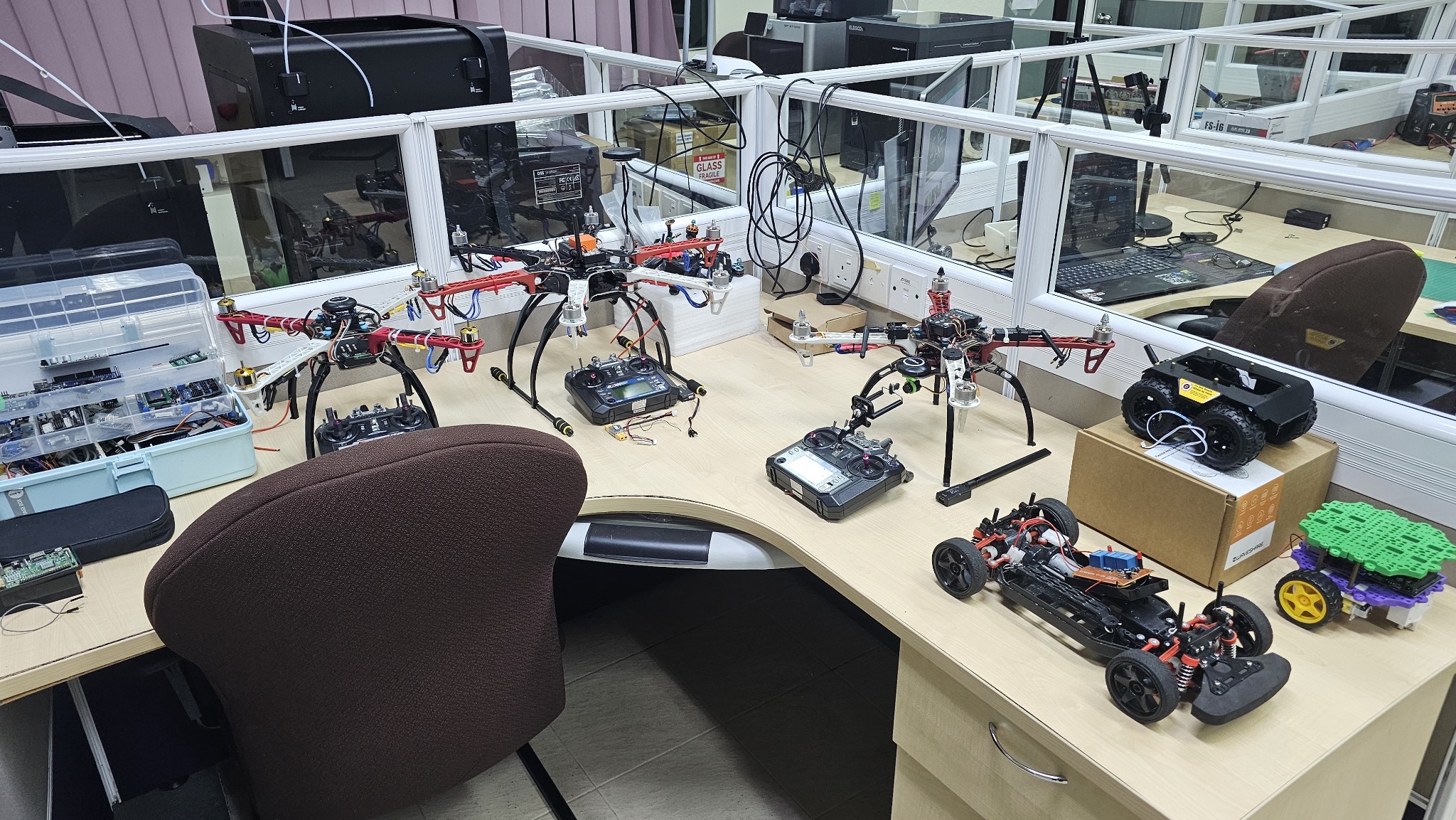
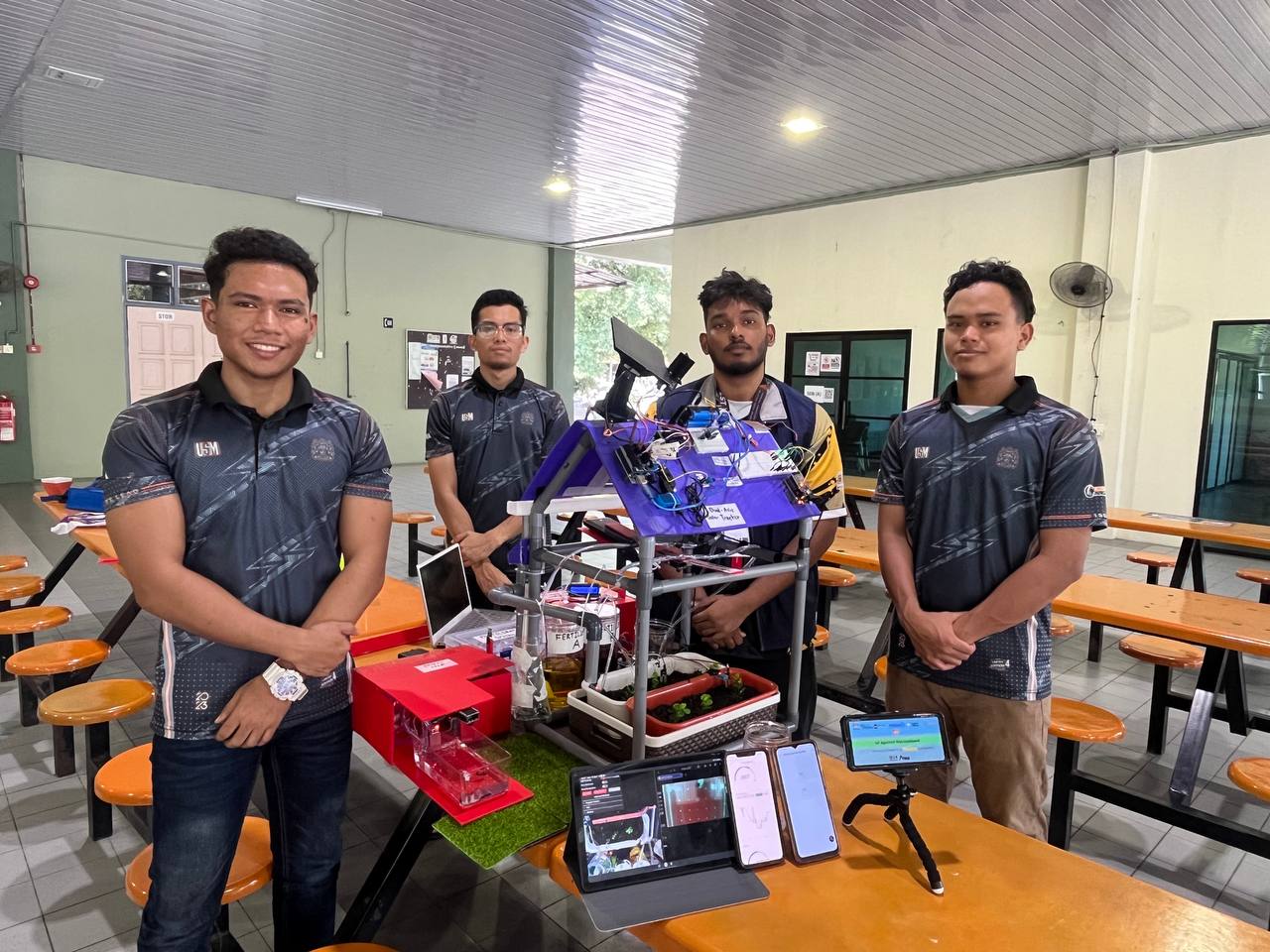
Illustrations demonstrate image placement. They are not photographs of Affan, completed project evidence, or earned credentials.

LAYOUT ENGINEERING PRINCIPLES

Care in every
layout decision.

The habits I aim to bring to every layout: understand the circuit, preserve design intent, verify changes and learn from review.

Tap a principle to see how it applies to the work.

Explore the principles Circuit First

Contact

Let’s talk about chips and robots!

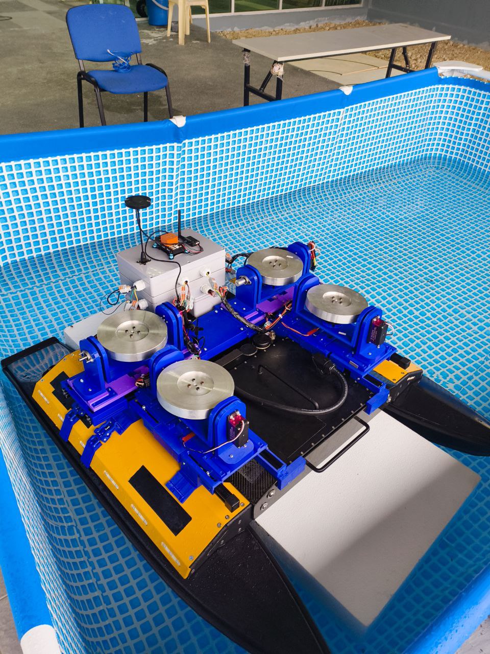
I’m Affan Iman, a Mechatronics graduate building my career in custom IC layout. My interests also span unmanned robotics, embedded systems, and hands-on engineering projects. If you’d like to discuss an opportunity, exchange ideas, or collaborate on a project, I’d be happy to connect.

fannximan@gmail.com

Affan Iman Penang, Malaysia

INTERACTIVE SILICON LAB

Silicon Explorer.

WAFER GEOMETRYInteractive semiconductor model; explanations and controls are below.
Educational model · dimensions simplified
Wafer & die footprint
0%